$2.4 Million Grant Gives Big Boost to Atomic-Level Manufacturing Project
By: Melissa Cutler | March 4, 2019

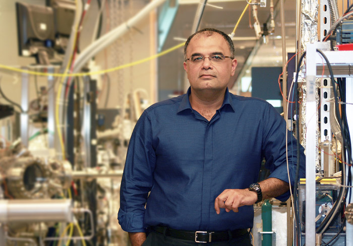
Dr. Reza Moheimani, professor of systems engineering at UT Dallas, and his team are developing microelectromechanical systems actuators, each equipped with an atomically sharp tip that could function as a scanning tunneling microscope.
Dr. Reza Moheimani, professor of systems engineering at The University of Texas at Dallas, recently received a $2.4 million grant from the U.S. Department of Energy to develop a platform technology for high-throughput, atomically precise manufacturing (APM).
The grant builds on innovative work led by Moheimani in scanning tunneling microscopy. Moheimani, who holds the James Von Ehr Distinguished Chair in Science and Technology, aims to develop enabling technologies for a novel approach to atomically precise manufacturing, which is essentially a form of 3D printing with atomic precision.
“Professor Moheimani’s team is developing groundbreaking advances in scanning probe technology that essentially make products virtually without defects — down to every atom,” said David Forrest, program manager in the Advanced Manufacturing Office at the Department of Energy (DOE). “The traditional speed of operation of these scanning probes currently prevents meaningful production rates. However, Professor Moheimani’s innovations break through longstanding barriers, with the potential for a thousandfold increase in speed and parallelization.”
“Professor Moheimani’s team is developing groundbreaking advances in scanning probe technology that essentially make products virtually without defects — down to every atom.”
David Forrest, program manager in the Advanced Manufacturing Office at the U.S. Department of Energy
The grant, which also involves Zyvex Labs and the National Institute of Standards and Technology, supports the development of new hardware and control algorithms to increase the speed and throughput of Moheimani’s APM method, scaling up the process to meet industry needs. New materials created by his APM approach have potential applications ranging from atomically precise membranes for removing minerals from water to emerging quantum computing circuits and two-dimensional quantum metamaterials.
“Reza is a scientist who particularly excels at bridging control theory and microelectromechanical systems devices very well, particularly in control systems for microminiature mechanical devices,” said Dr. Poras T. Balsara, interim dean of the Erik Jonsson School of Engineering and Computer Science. “I am not surprised that the DOE entrusted Reza with this grant for early-state, innovative technologies and solutions for advanced manufacturing.”
In 2017, Moheimani solved a 35-year-old problem: How to prevent the tip of a scanning tunneling microscope (STM) from crashing into the surface of a material during imaging or lithography.
STMs operate in an ultra-high vacuum, bringing a fine-tipped conductive probe with a single atom at its apex very close to the surface of a sample. When a voltage difference is established between the two objects, electrons can transfer across the gap between the tip and the sample, a quantum mechanical phenomenon known as “tunneling.”
Conventionally, the STM is used to image the surfaces of materials with atomic resolution. The STM is an extremely slow tool that uses a single tip to image or manipulate atoms on a surface. It uses a large piezoelectric actuator to position the micron-sized tip relative to the surface.
Moheimani’s group is developing microelectromechanical systems (MEMS) actuators, each a fraction of an inch in size and equipped with an atomically sharp tip that could function as a high-speed STM. These MEMS STMs can be scaled up in large arrays to enable high-throughput lithography for atomically precise manufacturing of novel materials and quantum electronic devices.

This micrograph taken with a scanning electron microscope shows an array of five atomic force microscopy microcantilevers, each with an atomically sharp tip (inset) that can be used to image and manipulate material surfaces with atomic resolution with the ultimate goal of creating new materials atom by atom. The measurements are in micrometers.
Moheimani and his collaborators use the STM to draw atomically precise patterns on hydrogen-terminated silicon surfaces by selectively removing hydrogen atoms. These vacancies can then be filled with other species of atoms to enable layer-by-layer fabrication with atomic precision and no defects.
“It is much like an atomically sharp needle,” Moheimani said. “The microscope itself functions like a robotic arm that can pluck atoms on the sample surface and manipulate them. Using this technology, we are able to build new, extraordinary materials atom by atom.”
Moheimani said that to make APM more commercially viable, a company would need thousands of STM tips, each with dedicated actuators and servo control loops that can move the tips in unison in various directions with atomic precision.
That’s not easy.
“It’s really hard to increase the size and scope of atomically precise manufacturing,” Moheimani said. “We don’t have to solve just one problem; we have to solve a dozen challenging problems and develop new systems and feedback control methods. Then we must put them together to get them to work simultaneously.”
Media Contact:
Melissa Cutler, UT Dallas, 972-883-4319, melissa.cutler@utdallas.edu, or the Office of Media Relations, UT Dallas, (972) 883-2155, newscenter@utdallas.edu.


