Quantum computers have the potential to transform fields such as medicine, cybersecurity and artificial intelligence by solving hard optimization problems that are beyond the reach of conventional computing hardware.
But the technology to manufacture the devices on a large scale does not yet exist.
Researchers at The University of Texas at Dallas have developed a technique that could remove one of the challenges to scaling the production of silicon quantum devices. The researchers outlined their method, which provides greater control and precision during the fabrication process, in a study published online May 28 and in the July print edition of the Journal of Vacuum Science & Technology B. Silicon is the preferred material for the base of quantum devices because of its compatibility with conventional semiconductor technology.
The study’s corresponding author, Dr. Reza Moheimani, the James Von Ehr Distinguished Chair in Science and Technology and a professor of systems engineering in the Erik Jonsson School of Engineering and Computer Science, received a $2.4 million U.S. Department of Energy grant in 2019 to develop technology for atomically precise manufacturing, the process of building new materials and devices atom by atom.
Moheimani’s team is addressing a range of challenges to quantum device fabrication.
“Our latest work increases the precision of the fabrication process,” Moheimani said. “We’re also working to increase throughput, speed and reliability.”
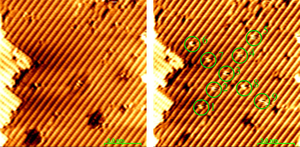
The researchers’ method for building a silicon-based qubit, or quantum bit, the basic unit of information in a quantum computer, starts with an atomically flat silicon surface coated with a layer of hydrogen, which prevents other atoms or molecules from getting absorbed into the surface. Next, researchers use a scanning tunneling microscope (STM), which features a probe with an atomically sharp tip, functioning as a micro-robotic arm, to remove atoms of hydrogen selectively from the surface. The STM was designed for imaging atomic features on a surface, however, researchers also use the device to manipulate atoms in a mode called hydrogen depassivation lithography (HDL).

“We realized that we could actually use this method to remove hydrogen atoms in a controlled fashion. This came as a surprise. It’s one of those things that happens during experiments, and you try to explain it and take advantage of it.”
Dr. Reza Moheimani, the James Von Ehr Distinguished Chair in Science and Technology in the Erik Jonsson School of Engineering and Computer Science
The painstaking process involves positioning the tip over an atom of hydrogen, adding a high-frequency signal to the tip-sample bias voltage and ramping up the amplitude of the high-frequency signal until the atom of hydrogen detaches from the surface, revealing silicon underneath. After a predetermined number of hydrogen atoms are selectively removed from the surface, phosphine gas is introduced in the environment and after a specific process, atoms of phosphorus are adsorbed to the surface, where each functions as a qubit.
The problem with conventional HDL is that it can be easy for the operator to pluck the wrong atom of hydrogen resulting in creation of qubits at unwanted locations. Using the STM for HDL requires a higher voltage than for imaging, which too often causes the tip to crash into the surface sample, forcing the operator to start over.
The researchers were working on their solution to the STM tip-crash problem when they discovered a more precise method for manipulating the surface atoms.
“Conventional lithography cannot achieve the requisite atomic precision,” Moheimani said. “The issue is that we are using a microscope to do lithography; we’re using a device to do something it’s not designed for.”
The researchers found that they could achieve higher precision by performing HDL in imaging mode, rather than the conventional lithography mode, with some adjustments to the voltage and a change to the STM’s feedback control system.
“We realized that we could actually use this method to remove hydrogen atoms in a controlled fashion,” Moheimani said. “This came as a surprise. It’s one of those things that happens during experiments, and you try to explain it and take advantage of it.”

Quantum computers are expected to be able to store more information than current computers. Current transistors, which relay information, cannot be made any smaller, said Hamed Alemansour, a mechanical engineering doctoral student and lead author of the study.
“The kind of technology that’s used now for making transistors has reached its limit. It’s difficult to decrease the size any more through conventional methods,” Alemansour said.
While a conventional computer uses the precise values of 1s and 0s to make calculations, the fundamental logic units of a quantum computer are more fluid, with values that can exist as a combination of 1s and 0s at the same time or anywhere in between. The fact that a qubit can represent two numbers at the same time allows the quantum computer to process information much faster.
One of the next challenges, Moheimani said, will be to develop technology to operate multiple STM tips at a time.
“What if we can use 10 or 100 tips in parallel with each other so we can do the same lithography multiplied by 100 times? What if we can do it 10 times faster? If we can manufacture 100 qubits 10 times faster, we’re 1,000 times better off already,” Moheimani said.
Other researchers involved with the current study include scientists at Richardson, Texas-based nanotechnology company Zyvex Labs: Dr. John Randall, president and CEO, who co-chairs the Jonsson School’s Industrial Advisory Council and is on the adjunct faculty at UT Dallas; Dr. James Owen, director of atomically precise manufacturing; and Dr. Ehud Fuchs, research scientist.